Nanocrystalline metals are metals with grain sizes on the nanometer scale, typical grain diameters range from 5 to 50 nanometers. These materials are of technological interest, mainly because their strength and hardness often are far above what is seen in coarse-grained metals. This is generally believed to be caused by the grain boundaries acting as barriers to dislocation motion: as the grain size is decreased, the number of grain boundaries increase and the dislocation motion becomes harder, leading to a harder material. This grain size dependence of the hardness and the yield stress -- the Hall-Petch effect (Hall 1951; Petch 1953) -- is observed in coarse grained materials as well as in nanocrystalline metals. It is indeed possible to get a good estimate of the hardness of nanocrystalline metals by extrapolating from the Hall-Petch behaviour at larger grain sizes. For a further discussion of the mechanical properties of nanocrystalline metals, see e.g. the reviews by Siegel and Fougere (1994) or Morris and Morris (1997).
Nanocrystalline metals are an attractive group of materials to model for many reasons. The materials are interesting from a technological point of view, but also from a theoretical point of view since the small grain size results in a ``cut off'' of the typical length scales of the phenomena and structures that may appear during the deformation process. This simplifies the deformation process and may possibly facilitate the development of theoretical models. Eventually, it may be possible to extend these models to the more complicated cases of coarse grained materials. For the smallest grain sizes (below approximately 5-10nm) it becomes possible to model the deformation process directly using atomic-scale computer simulations. The deformation processes may then be studied directly (Schiøtz, Di Tolla and Jacobsen 1998; Van Swygenhoven and Caro 1997a,b).
We attempt to generate ``samples'' with a structure reasonably similar
to the structures observed experimentally: essentially equiaxed
dislocation free grains separated by narrow grain boundaries. The
grains are produced using a Voronoi construction. A set of
grain centres are chosen randomly, and the part of space closer to a
given centre than to any other centre is filled with atoms in a
randomly rotated f.c.c. lattice. Periodic boundary conditions are
imposed. This procedure generates samples without texture, and with
random grain boundaries. In the grain boundaries thus generated, it
is possible that two atoms from two different grains get too close to
each other, in such cases one of the atoms is removed to prevent
unphysically large energies and forces as the simulation is started.
To obtain more relaxed grain boundaries the system is annealed for
10000 timesteps (50ps) at 300K, followed by an energy
minimisation. This procedure is important to allow unfavourable local
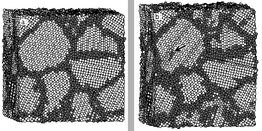
atomic configurations to relax. A sample generated in this way is
shown in Fig. 1.
 |
To investigate whether the parameters of the annealing procedure are critical, we have annealed the same sample for 50 and 100ps at 300K, and for 50ps at 600K. We have compared the mechanical properties of these samples with those of an identical sample without annealing, we find that the annealing is important (the unannealed sample was softer), but the parameters of the annealing are not important within the parameter space investigated.
A similar generation procedure has been reported by Chen (1995), by D'Agostino and Van Swygenhoven (1996), and by Van Swygenhoven and Caro (1997a,b). A different approach was proposed by Phillpot, Wolf and Gleiter (1995a,b): a nanocrystalline metal is generated by a computer simulation where a liquid is solidified in the presence of crystal nuclei, i.e. small spheres of atoms held fixed in crystalline positions. The system was then quenched, and the liquid crystallised around the seeds, thus creating a nanocrystalline metal. In the reported simulations, the positions and orientations of the seeds were deterministically chosen to produce eight grains of equal size and with known grain boundaries, but the method can naturally be modified to allow randomly placed and oriented seeds. The main drawback of this procedure is the large number of defects (mainly stacking faults) introduced in the grains by the rapid solidification. The stacking faults are clearly seen in the resulting nanocrystalline metal (Fig. 7 of Phillpot et al. 1995a). Some of us have earlier performed simulations of the solidification of a large cluster (unpublished). These simulations have shown that a large number of stacking faults appear even if the cooling is done as as slowly as possible in atomistic simulations.
We model the interactions between the atoms using a many-body potential known as the Effective Medium Theory (EMT) (Jacobsen, Nørskov and Puska 1987; Jacobsen, Stoltze and Nørskov 1996). It is very important that the interactions are modelled using a realistic many-body potential such as EMT, the Embedded Atom Method (Daw and Baskes 1984) or the Finnis-Sinclair model (Finnis and Sinclair 1984, 1986). Pair potentials such as Lennard-Jones are still seen used for simulating metals due to the lower computational burden.1 Although they give a good description of noble gas solid, they are not adequate for modelling the bonding in metallic systems. One symptom of this is seen in the elastic constants, all pair potentials result in materials that satisfies the Cauchy relations between the elastic constants ( C12 = C44 for cubic crystals), a relation that is far from true in most metals.
In the simulations, the samples are deformed by slowly increasing the system size along the z axis while minimising the energy with respect to all atomic coordinates and with respect to the box dimensions in the x and y directions. The minimisation is done as a modified molecular dynamics simulation. After each timestep the dot product between the momentum and the force is calculated for each atom. Any atom where the dot product is negative gets its momentum zeroed, as it is moving in a direction where the potential energy is increasing. This MDmin algorithm (Stoltze 1997) is very efficient for this type of minimisation. Before each timestep, the system is stretched a little along the z direction. The two lateral dimensions are optimised by a Monte Carlo procedure: every 20 timesteps a change in the dimensions is proposed, if the change results in a lower energy it is accepted, otherwise it is discarded. A few simulations were performed using the conjugate gradient algorithm for energy minimisation (Press, Flannery, Teukolsky and Vetterling 1988). The two algorithms were approximately equally efficient.
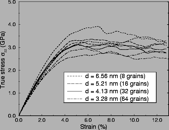
During the simulation, the local stresses were calculated and stored
for further analysis, and the global values of the stress tensor were
stored to generate stress-strain curves. A set of stress-strain
curves is shown in Fig. 2.
 |
To facilitate the analysis of the simulations, the local order in the sample was analysed. This was done using a method called Common Neighbour Analysis (Jónsson and Andersen 1988; Clark and Jónsson 1993). By investigating the bonds between the neighbouring atoms to the atom under investigation, the local crystal structure is determined. Atoms are then classified into three classes. Atoms in a local f.c.c. order are considered ordinary bulk atoms; atoms in local h.c.p. order are labelled as belonging to a stacking fault or the like; and atoms in all other local orders are considered part of the grain boundaries or of dislocation cores. This classification can be seen in Fig. 1.
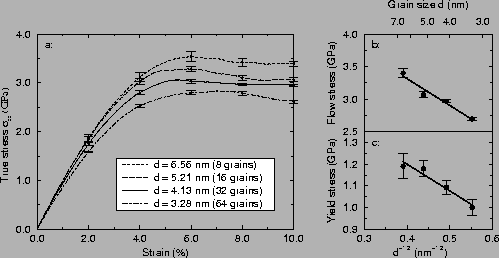
Fig. 3a shows the average stress-strain curves at
each grain size. A clear grain size dependence is seen in the maximal
flow stress. Fig. 3b and c summarise the results,
showing the maximal flow stress and the 0.2% offset yield stress in a
standard Hall-Petch plot, i.e. as a function of one over the square
root of the grain size. A reverse Hall-Petch effect is clearly seen,
it will be discussed in section 3.
 |
In Fig. 1b stacking faults are present in several grains. They are created as partial dislocations (Shockley partials) move through the grains. They would be removed if a second partial dislocation followed in the same plane. This is, however, rarely seen, possibly because the grain size is comparable to the splitting width of the dislocation. Simulations of dislocation emission from a notch in a surface (Schiøtz, Jacobsen and Nielsen 1995) have shown that the leading partial will move several splitting widths away from the notch, before the trailing partial is emitted. Possibly a similar effect is seen here.
We have measured the amount of dislocation activity in the systems.
The total dislocation activity is able to explain at most 2-3%
plastic deformation, i.e. less than half the observed plastic
deformation. To identify the nature of the remaining deformation, we
analysed the relative motion of the individual atoms.
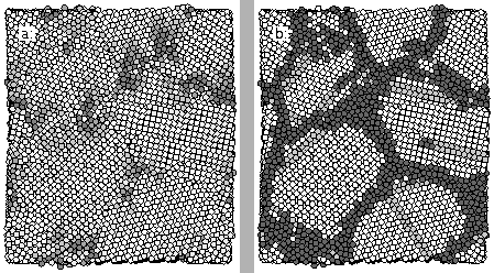
Fig. 4a shows the magnitude of the motion of the atoms
obtained by subtracting the coordinates at two different strains
(differing by 0.4%). The collective motion due to the imposed strain
rate has been subtracted out. Darker atoms move most. By comparing
with Fig. 4b showing the positions of the grain
boundaries, it is seen that the motion occurs mainly in the grain
boundaries. An indication of the activity in the grain boundaries can
also be seen in Fig. 1: the grain boundaries have
become a little thicker during deformation.
 |