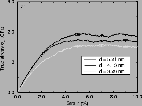
As is seen in Fig. 3, a reverse Hall-Petch effect is observed in the simulations, i.e. the material gets softer as the grain size is decreased. This is opposite of the normally seen behaviour, but has occasionally been observed experimentally in nanocrystalline materials with sufficiently small grain sizes (Chokshi, Rosen, Karch, Gleiter 1989). There are also observations of ``kinked'' Hall-Petch graphs, i.e. cases where the slope is reduced (but still positive) below a certain grain size. Many explanations have been proposed, of which some are summarised below. The explanations are not necessarily mutually exclusive, nor is it unlikely that different explanations may apply depending on the way the material was produced. It seems reasonable to assume that the deformation mechanism is different in samples produced by e.g. inert gas condensation, producing essentially dislocation-free grains, and by severe plastic deformation, where the small grains are produced by breaking up larger grains through intense dislocation activity. The most commonly proposed explanations are increased diffusional creep, suppression of dislocation pileups, different grain boundary structures, poor sample quality (porosity and other flaws), and deformation in the grain boundaries.
Chokshi et al. (1989) propose that the reverse Hall-Petch effect is caused by enhanced Coble creep, i.e. creep due to diffusion in the grain boundaries. Coble creep scales with the grain size (d) as d-3, and estimates of the creep rate of nanocrystalline metals indicate that this could be the explanation of the reverse Hall-Petch effect. Direct measurements of the creep rate have, however, ruled out this explanation (Nieman, Weertman and Siegel 1990; Nieh and Wadsworth 1991).
The Hall-Petch effect is normally explained by appealing to dislocation pileups near the grain boundaries. Once the grain size drops below the equilibrium distance between dislocations in a pileup, pileups are no longer possible, and the Hall-Petch relation should cease to be valid (Nieh and Wadsworth 1991; Pande, Masumura and Armstrong 1993). It is, however, not clear how the yield stress should depend on the grain size below that point. The critical grain size is estimated to be 20nm for copper (Nieh and Wadsworth 1991).
Is is not unreasonable to assume that the grain boundary structure might be different when the grain size is very small (Zhu, Birringer, Herr and Gleiter, 1987). It has been proposed that grain boundaries in nanocrystalline metals may be more ``transparent'' to dislocations, and thus allow dislocations to run through several grains (Valiev, Chmelik, Bordeaux, Kapelski and Baudelet 1992; Lian, Baudelet and Nazarov 1993; Lu and Sui 1993). This was proposed in connection with measurements of a possible breakdown of the Hall-Petch relation in metals with sub-micrometer grain sizes, produced by severe plastic deformation (Valiev et al. 1992). Recent high-resolution electron microscopy studies show, that the grain boundaries in metals produced in this way have a complex structure, with a large number of dislocations very close to the grain boundary (Horita, Smith, Furukawa, Nemoto, Valiev and Langdon 1996). This should make the grain boundaries less transparent to dislocations, but a change in slope in the Hall-Petch relation is seen at grain sizes below 100nm (Furukawa, Horita, Nemoto, Valiev and Langdon 1996). They explain the change as enhanced plasticity due to these extra dislocations near the grain boundaries.
Many of the observations of a reverse Hall-Petch effect are from samples generated using inert gas condensation, where a large number of nanometer-sized clusters are compacted to produce the sample. If the compaction is not complete, small voids will be present between the grains. The presence of these voids was not initially recognised, the lower density being ascribed to special low-density grain boundaries. If the nanocrystalline metal contains a significant volume fraction of porosity, this will obviously reduce the hardness significantly. Surface defects alone have been shown to be able to reduce the strength of nanocrystalline metals by a factor of five (Nieman, Weertman and Siegel 1991; Weertman 1993).
Many of the early measurements of a reverse Hall-Petch effect are likely to have been caused by unrecognised porosity in the samples. Improved techniques (Sanders, Fougere, Thompson, Eastman and Weertman 1997) have allowed production of nanocrystalline samples with densities above 98%, these have shown no reverse Hall-Petch effect in copper at grain sized down to approximately 10-15nm (Sanders, Youngdahl and Weertman 1997).
As the grain size is reduced, the volume fraction of the grain boundaries increase, and it is reasonable to assume that at some point they will begin to play a role in the deformation process. Li, Sun and Wang (1994) propose a deformation mechanism based on motion of grain boundary dislocations.
Computer simulations give a possibility to distinguish between this
large number of different explanations. The computer simulations
presented here clearly indicate that a new deformation mechanism
becomes active in the grain boundaries (Schiøtz et al. 1998). It
does not appear to be a grain boundary dislocation based motion, but
rather a large number of small events, where only a few atoms (or a
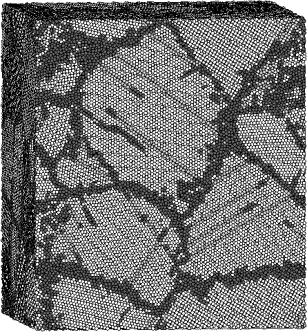
few tens of atoms) move simultaneously (Fig. 4). This
produces a large number of small, apparently uncorrelated slipping
events in the grain boundaries, leading to grain boundary sliding.
The processes also lead to the grain boundaries becoming thicker
(Fig. 1). This does, however, seem to be a
result of doing the simulations at zero temperature. Simulations at
room temperature do not result in a change in the grain boundary
thickness, otherwise the results are very similar apart from a
reduction of the yield and flow stresses due to increased grain
boundary sliding (Fig. 5).
 |
Simulations of nanocrystalline nickel also show that the main deformation mechanism is grain boundary sliding and grain boundary motion, where one grain grows at the expense of another (Van Swygenhoven and Caro, 1997a,b). Those simulations are stress controlled, i.e. the stress is controlled, and the strain is measured, contrary to the simulations reported here, which are strain controlled. The strain rate was measured as a function of grain size, giving a higher strain rate at lower grain boundaries, consistent with a viscoelastic behaviour of the grain boundaries (Van Swygenhoven and Caro, 1997b).
Simulations of the sintering of nanocrystalline Cu particles to form a fully dense nanocrystalline sample also indicate that the main deformation is in the grain boundaries (Zhu and Averback, 1996).
The observations of a reverse Hall-Petch effect in the simulations
presented here are not in conflict with the experiments reported by
Sanders et al. (1997), since the experiments were
done on samples with grain sizes above 10-15nm. In order to
investigate if the transition between the normal and the reverse
Hall-Petch effect could be observed, a version of the simulation
program was written for parallel computers. This allowed us to
increase the number of atoms by a factor of ten, thus more than
doubling the grain size. Such a simulation is shown in
Fig. 6. Preliminary results indicate that the
reverse Hall-Petch effect persists at these grain sizes.
 |